Peruvian Engineers Develop Open-Source Chip

The design of integrated circuits is one of the main technological areas in science and engineering which has enabled the development of electronics in the last decades. Semiconductor foundries, which manufacture integrated circuits or chips, develop multiple technologies which are made available to circuit design companies through process design kits (PDKs) so that they can design these chips using their technologies. These PDKs are highly protected and only shared via non-disclosure agreements (NDAs). Thus, there is a barrier that limits accessibility to PDKs for circuit design purposes. This barrier only grows further after taking into account how expensive proprietary design tools are.
Recently, open-source integrated circuit design has gained more interest due to the release of the first open-source PDKs (Open-PDKs), the continue development of open-source design tools, and the potential of developing integrated circuits in a open ecosystem supported by the community. Basic circuits to characterize and continue the development of these Open-PDKs have been designed in recent years; the community of open-source chip designers has begun to grow significantly.
In this context, a team of engineers from the Pontifical Catholic University of Peru (PUCP) has designed and sent for fabrication the first open-source Peruvian chip. This chip implements a power management unit (PMU) which will be used as a building block of an application-specific integrated circuit (ASIC) targeting neural recording and modulation applications. This open-source ASIC will be included in a neural implant, which is a device that allows the direct interaction with the brain using an array of tiny electrodes for electrical sensing and stimulation. This device will be used for neuroscience and neuroengineering research, and further development of neural implants.
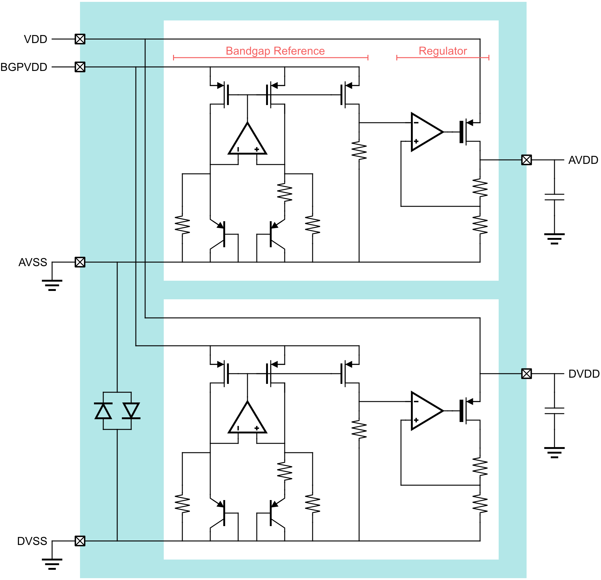
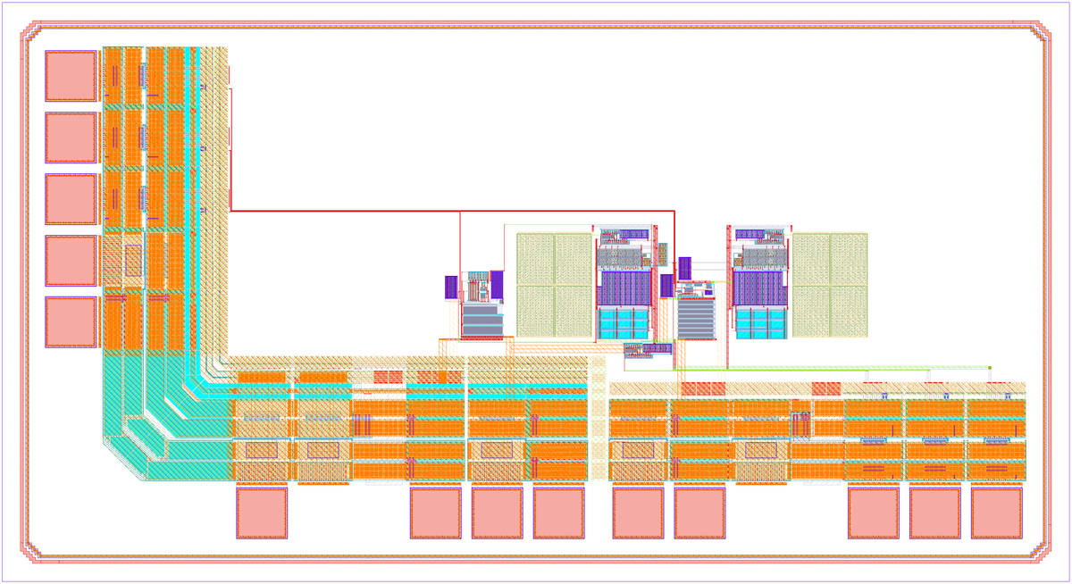
The PMU in the chip receives an input voltage within 1.4 V and 3.3 V and generates two regulated independent voltages of 1.2 V and 1.0 V to power the analog and digital circuits of the future ASIC, respectively. The PMU consists of two low-dropout regulators (LDOs) and two bandgap voltage references. The LDO consists of a transistor connected between the input and the output which regulates the output voltage through a negative feedback loop implemented with an operational amplifier. The bandgap voltage reference consists of a circuit topology which generates electrical currents independent of temperature and proportional to intrinsic Silicon properties such its bandgap. This chip has been designed in the130 nm IHP Open-PDK (The Leibniz Institute for High Performance Microelectronics) within its Open-Silicon-MPW program. The chip has a size of 1.5 mm x 0.8 mm. Figure 1 shows the simplified schematic of the chip and Figure 2 the chip layout. More details about the chip can be found in the GitHub repository.
Some of the participants of the Peruvian team are:
- Manuel Monge – Founder and CEO, OpenIC, US; Adjunct Professor, PUCP, Peru.
- Julio Saldaña – Adjunct Professor, PUCP, Peru.
- Massimo Bruschi – Electronic Engineer Student, Senior Year, PUCP, Peru.
Acknowledgements
- IHP for access to its Open-Silicon-MPW program.
- OpenIC for financial support.
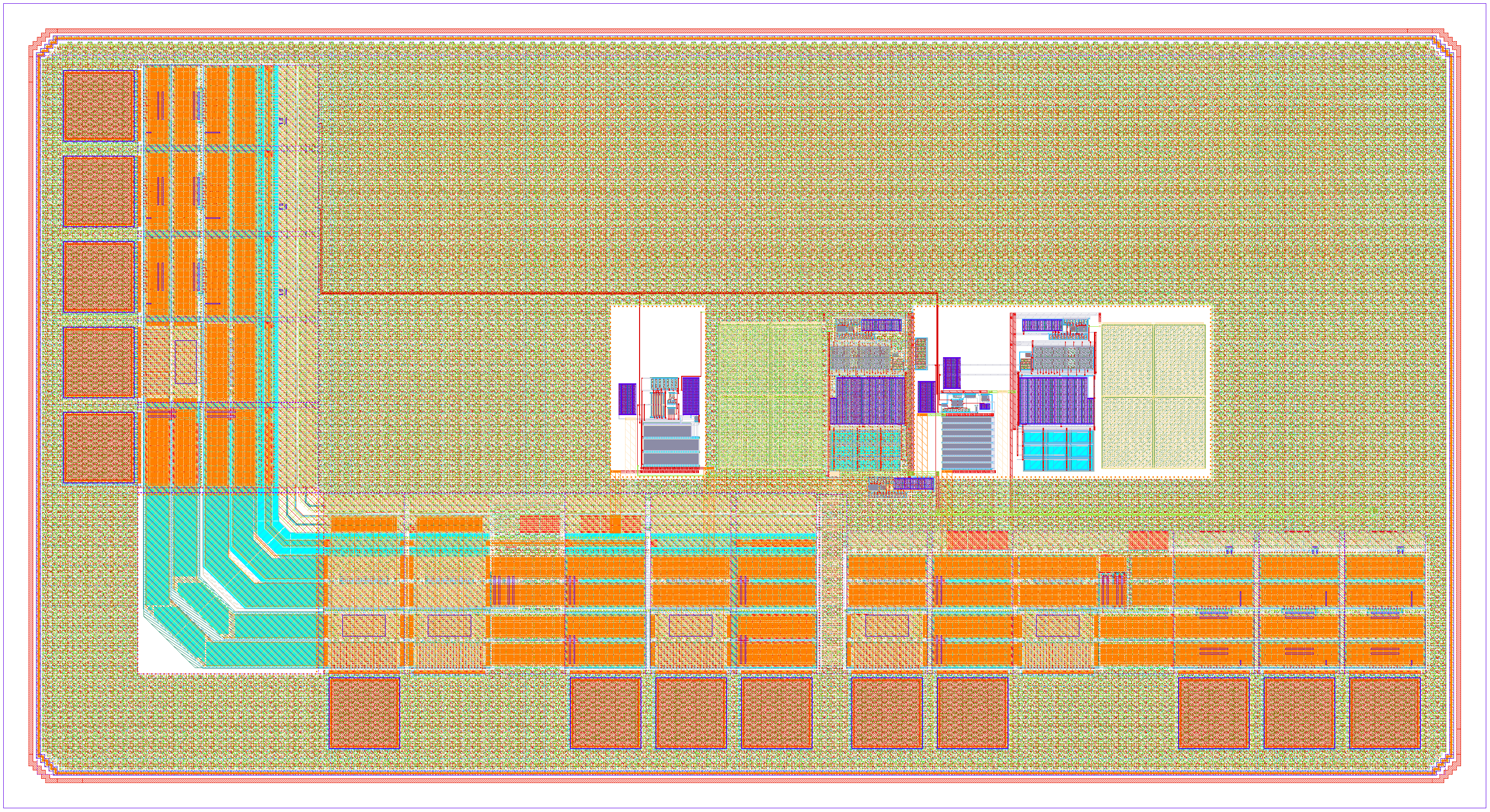

Figure 2.Layout of the chip with all necessary layers to be sent for fabrication (top) and without filler layers to highlight the circuits.
